Application
applicationFunction description
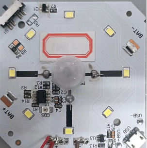
This plan is a lithium battery powered motion detection night light, which uses ULP ultra-low power motion detection chip HS6601L. The three modes of normally on, induction and off can be selected through the dial switch, and the sensitivity and timing time can be adjusted by adjusting the resistance parameters on the board.
Features
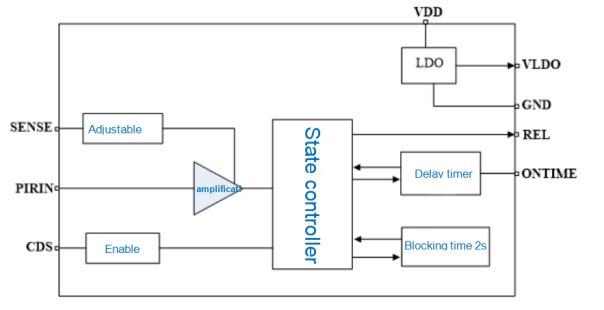
HS6601Lhas a built-in LDO, It can supply power to the probe and has strong stability.
Hs6601l is simple to use with no programming required, and the peripheral circuit is simple too.
The power consumption of HS6601l is only 20ua, which improves the endurance of the plan.
The sensing distance is adjustable and flexible.
Built in delay time timer, the delay time can be adjusted outside.
Physical drawing of the plan

Schematic diagram of the plan

Scheme function description
In this scheme, the charging of the battery is in the charge of a special charging management chip. When the third gear dial switch is turned to the first gear, the negative pole of the battery is connected to the VSS of the chip, and the chip starts to work to realize the sensing function;Turn to the second gear, the negative pole of the battery is connected to the negative pole of the lamp, and the lamp is always on;Turn to the third gear, the negative pole of the battery is disconnected, the chip and the lamp do not work, and enter the shutdown state. When in the induction mode, the photosensitive sensor will also be detected. When in the daytime, the chip will not sense the human signal and enter the standby state. When it detects the night, it will sense the human signal, the light threshold can be adjusted by adjusting the pull-up resistance R1 of the photosensitive sensor. If the light sensing function is not required, the photosensitive sensor can not be welded. The induction sensitivity can be adjusted by adjusting the R12 resistance. The smaller the R12 resistance, the more sensitive the induction is. The trigger time can be adjusted by adjusting R3 resistance. The smaller the R3 resistance, the shorter the trigger time.
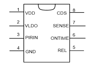
HS6601LFoot position description

pin | Name | I/O | Function description |
1 | VDD | P | Positive end of working power supply |
2 | VLDO | O | 2.7V LDO output |
3 | PIRIN | I | PIR Signal input terminal |
4 | GND | P | Negative end of working power supply |
5 | REL | O | Control signal output terminal, high level effective |
6 | ONTIME | I | Timing adjustment port |
7 | SENSE | I | Distance adjustment port |
8 | CDS | I | Optical control input port When CDS<0.5V, prohibit triggering ;CDS>1.0V, allow triggering |
HS6601LFunction diagram
